Brand: European & American
Product DetailsFAQInquire
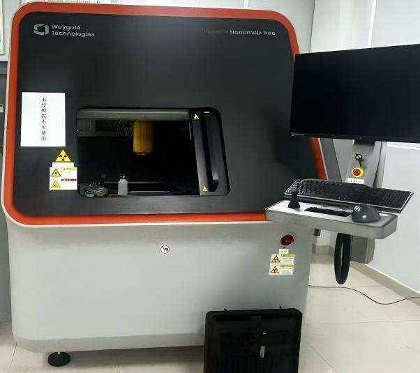
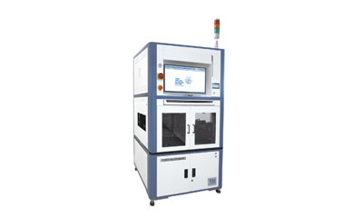
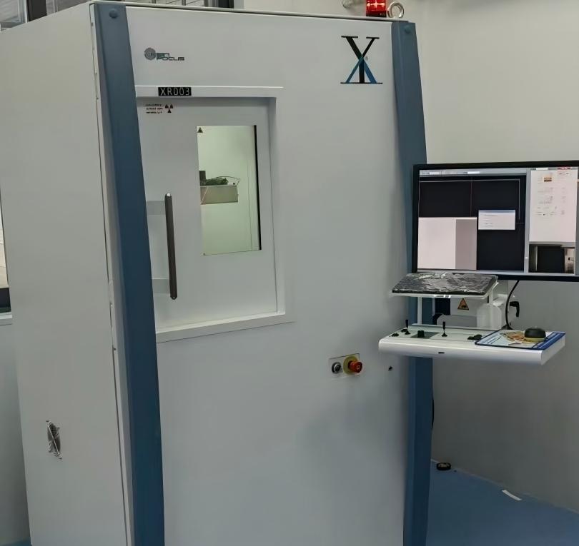
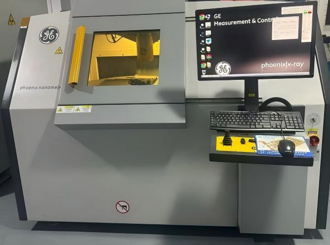
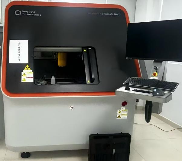
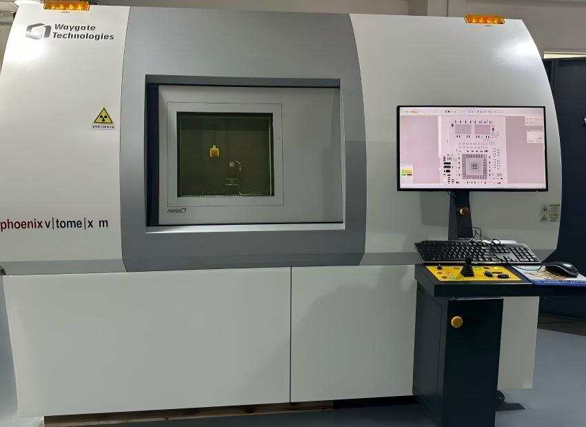
GE Phoenix Nanome|x Neo, Nanome|x Neo X-ray
High-Resolution Nanofocus X-Ray & 3D CT Inspection System for Semiconductor & Electronics
GE Phoenix Nanome|x Neo is a premium nanofocus X-Ray inspection system integrating 2D X-ray, Planar|CT and full 3D computed tomography in one platform, designed for non-destructive testing, failure analysis, R&D and quality control of advanced electronic assemblies, semiconductor packages, PCBs and lithium battery components.
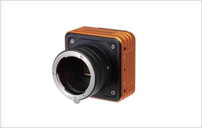
The Nanome|x Neo adopts 180kV / 20W high-performance nanofocus X-ray tube with diamond target window, paired with high dynamic cooled DXR flat panel detector. It delivers ultra-fine feature recognition and high magnification imaging to visualize hidden internal structures and micro-defects that cannot be captured by conventional optical inspection.
The Nanome|x Neo features Waygate’s diamond target nanofocus X-ray tube, delivering stable high-power output with excellent long-term focus stability. It achieves sub-micron resolution for microelectronic samples, supporting ultra-fine feature detection for advanced packaging. Equipped with active-cooled DXR flat panel detector, the system supports up to 30 fps live imaging and fast CT data acquisition. The built-in Flash!Filters™ image enhancement optimizes image contrast to reveal subtle defects.
Powered by Phoenix X|act inspection software, the system supports CAD-based µAXI automated inspection, easy programming, automatic BGA solder joint evaluation and multi-die attach void calculation. Typical capabilities include: CAD-based Automated µAXI, BGA Void Measurement, Die Void Analysis, Planar|CT for large PCB slicing, 3D NanoCT Scanning, Image Enhancement, Dimensional Measurement, Data Logging & Reporting
The Planar|CT function eliminates overlapping image artifacts for large PCBA, enabling clear slice imaging without cutting samples. Optional nanoCT® provides volumetric 3D reconstruction for internal structural analysis.
High-precision motion stage supports up to 70° oblique viewing angle, allowing operators to examine complex solder joints and stacked internal structures from multiple perspectives for comprehensive defect diagnosis.
Semiconductor Advanced Packaging, SMT / PCBA, BGA / CSP, Power Electronics, Automotive Electronics, Aerospace Electronics, Medical Electronics, Lithium-ion Battery Inspection, R&D & Failure Analysis
Solder Voids, BGA Voids, Die Attach Voids, Open Solder Joints, Solder Bridging, Insufficient Solder, Wire Bond Cracks, Package Cracks, Delamination, Internal Structural Defects, Battery Internal Defects
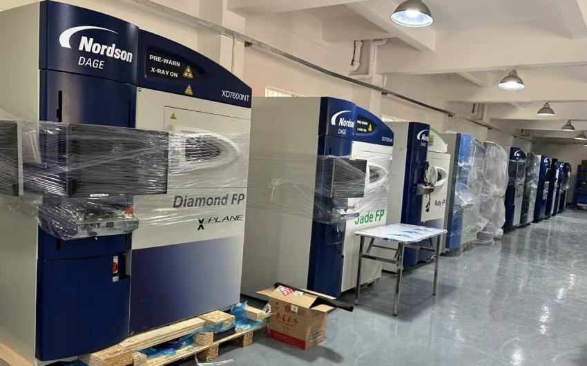
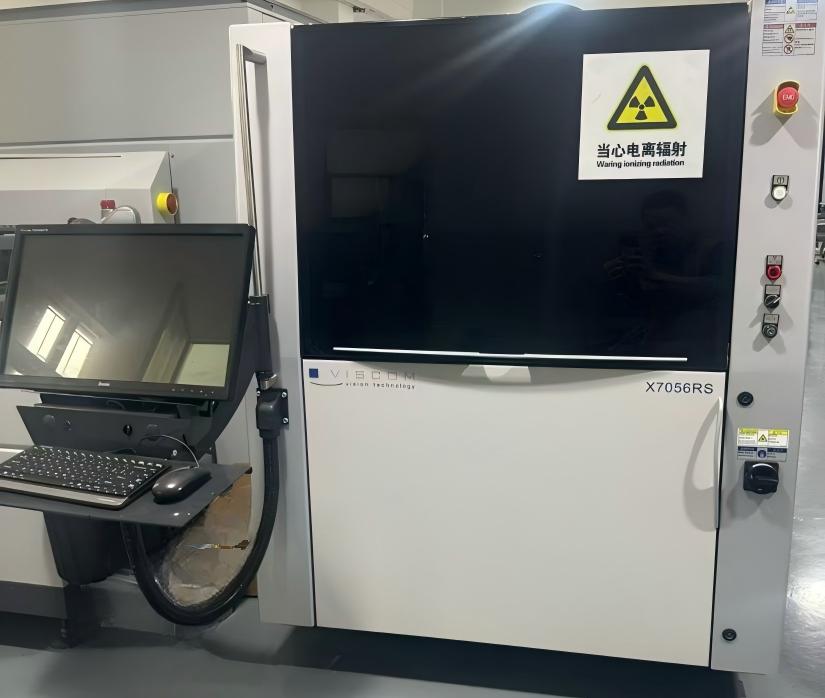
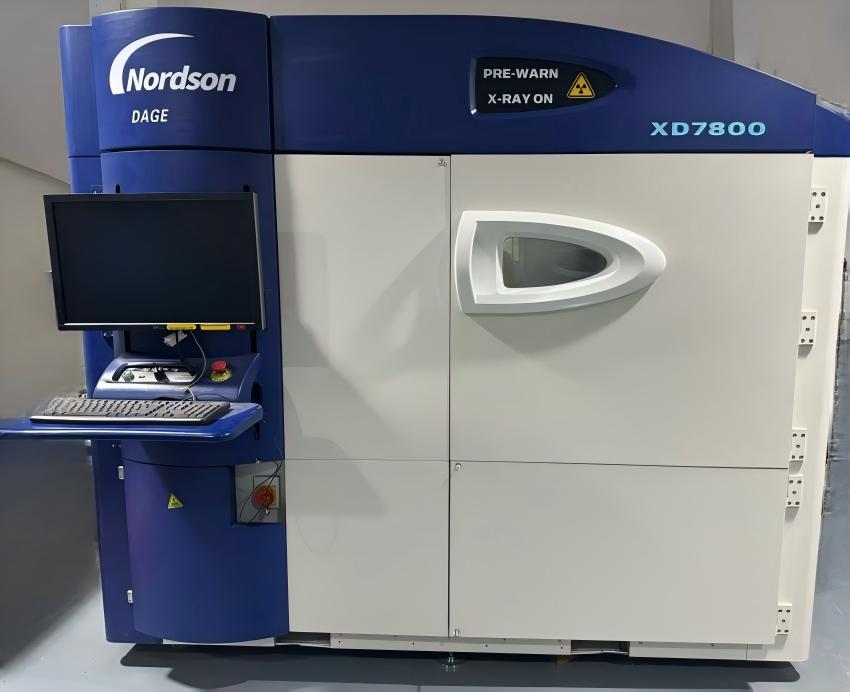
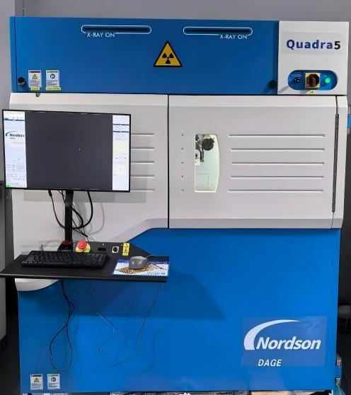
SMT Inspection World supplies pre-owned GE Phoenix Nanome|x Neo X-Ray and CT inspection systems for global semiconductor and electronics manufacturers. Prior to shipment, used units will go through professional inspection, functional testing and condition evaluation based on actual hardware configuration.
We also provide:
Equipment Sales, Used Equipment Trading, Equipment Rental, Installation & Commissioning, Maintenance, Spare Parts Supply, Equipment Upgrade, Technical Support

Specializing in brand new & used PARMI 3D Automatic Optical Inspection (AOI) and 3D Solder Paste Inspection (SPI) equipment sales, rental and genuine spare parts supply. With more than ten years of in-depth industry experience, we have served over 50 manufacturing enterprises at home and overseas.
All new and used devices are fully overhauled, precision-calibrated and functionally tested in strict accordance with original factory delivery standards. Every hardware component, software program and optical system is debugged item by item to ensure excellent operating stability and inspection accuracy. All equipment is fully production-ready and can be put into SMT line operation immediately after arrival.














 Wechat