Brand: European & American
Product DetailsFAQInquire
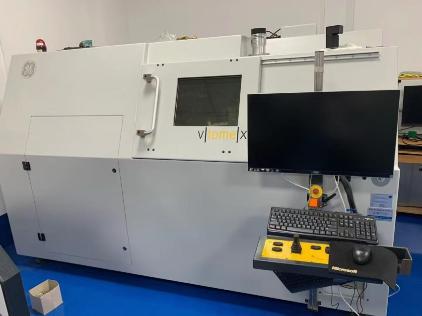
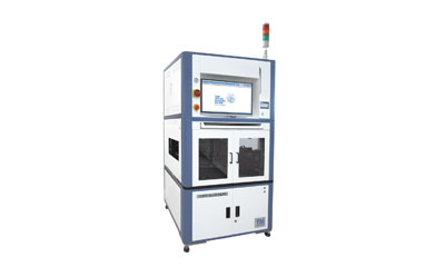
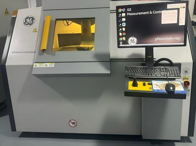
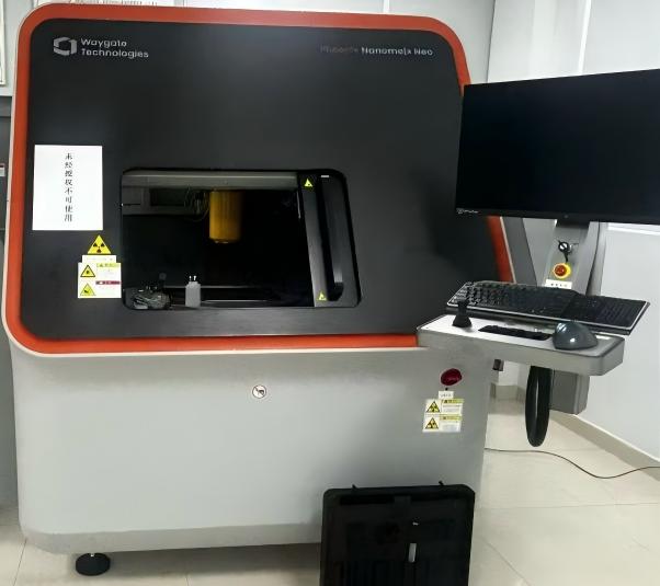
GE phoenix|x-ray nanome|x X-Ray Inspection System | Used Nanofocus X-Ray Equipment
GE phoenix|x-ray nanome|x is an ultra-high-resolution nanofocus X-Ray inspection system designed for advanced inspection of semiconductor packages, SMT assemblies, microelectronics and high-density electronic components.
Using high-power nanofocus X-Ray technology, the nanome|x provides detailed imaging of extremely small internal structures and hidden defects that are difficult or impossible to detect using conventional optical inspection. It is particularly suitable for BGA, CSP, Flip Chip, semiconductor packages, die attach and advanced electronic assemblies.
The phoenix|x-ray nanome|x uses high-power nanofocus X-Ray technology to achieve extremely high image resolution for microelectronic structures.
Historical specifications describe configurations with 180 kV / 15 W nanofocus X-Ray technology and detail detectability down to approximately 0.2 µm, depending on configuration.
The system is designed for applications requiring extremely detailed inspection of:
BGA、CSP、Micro-BGA、Flip Chip、Die Attach、Wire Bond、Semiconductor Packages、High-Density PCBA
It can be used for process control, quality inspection, failure analysis and R&D applications.
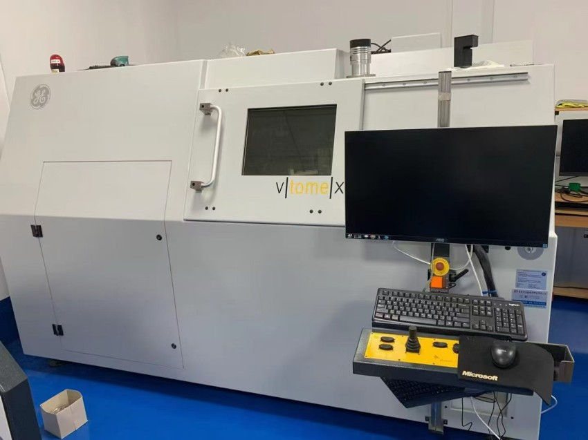
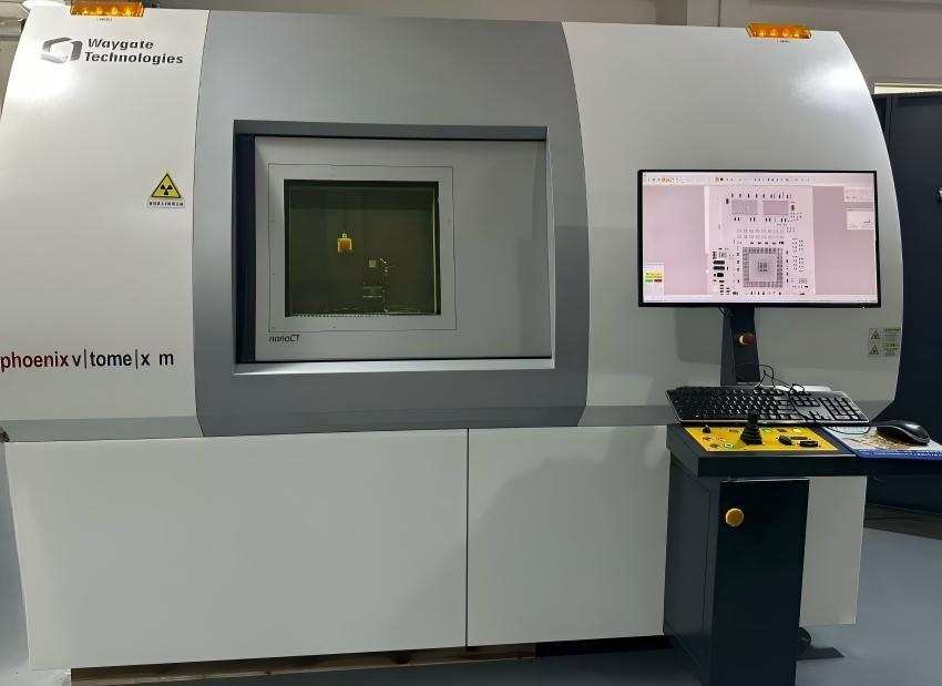
The nanome|x can be upgraded with nanoCT® technology for high-resolution three-dimensional inspection.
3D CT allows engineers to visualize internal structures and analyze defects such as die-attach voids, cracks, bonding defects and complex semiconductor package structures without destroying the sample.
The system can also support CAD-based µAXI inspection, allowing automated inspection routines for high-resolution applications and improving inspection repeatability and defect coverage.
Semiconductor Packaging、Advanced Packaging、SMT / PCBA、BGA / CSP、Flip Chip、Die Attach、Wire Bond、Microelectronics、Automotive Electronics、Medical Electronics、Aerospace Electronics、High-Reliability Electronics
Solder Voids、BGA Voids、Die-Attach Voids、Wire Bond Defects、Cracks、Delamination、Open / Short、Solder Bridging、Internal Structural Defects
SMT Inspection World provides used GE phoenix|x-ray nanome|x X-Ray inspection systems for electronics and semiconductor manufacturers worldwide.
Used equipment can be professionally inspected, functionally tested and evaluated according to its actual configuration and operating condition before delivery.
We also provide:
Used Equipment Sales、Equipment Rental、Installation & Commissioning、Equipment Maintenance、Spare Parts Supply、Equipment Upgrade、Technical Support

Specializing in brand new & used PARMI 3D Automatic Optical Inspection (AOI) and 3D Solder Paste Inspection (SPI) equipment sales, rental and genuine spare parts supply. With more than ten years of in-depth industry experience, we have served over 50 manufacturing enterprises at home and overseas.
All new and used devices are fully overhauled, precision-calibrated and functionally tested in strict accordance with original factory delivery standards. Every hardware component, software program and optical system is debugged item by item to ensure excellent operating stability and inspection accuracy. All equipment is fully production-ready and can be put into SMT line operation immediately after arrival.











 Wechat